Hands-on Microfabrication for Integrated Circuits
(A limited enrollment 6-week IC Fabrication Training Course)
Table of Contents
Course Description:
This is a comprehensive 6-week IC fabrication short course meticulously designed to bridge the gap between theoretical knowledge and practical application in the dynamic world of semiconductor technology.
This intensive program uniquely integrates the critical phases of integrated circuit development:
- Design
- Pre-fabrication
- Fabrication
- Testing
Participants will gain invaluable hands-on experience with semiconductor processes within a cleanroom fab lab, culminating in the production and characterization of functional CMOS circuits.
Passionate about semiconductor technology?
This course equips you with the essential skills and industry insights to thrive in a rapidly evolving industry.
Beyond academic rigor, the program emphasizes real-world industry relevance by providing unmatched exposure to the intricacies of IC fabrication and its impact on the global technology landscape.
Who Should Attend?
The program is designed for:
- Aspiring Semiconductor Professionals: This course is ideally suited for students in the completion phase of their undergraduate degrees in Electronics and Electrical Engineering, or related disciplines, who are eager to launch careers in the semiconductor industry.
It provides a significant competitive advantage by offering practical fabrication experience often lacking in traditional curricula, equipping you with hands-on skills in photolithography, thin film deposition, and etching, making you highly competitive for entry-level positions in fabrication, process engineering, or design roles. - Graduate Students and Researchers: Graduate students in microelectronics, nanotechnology, and related fields will find this course highly beneficial for deepening their understanding of fabrication processes and enhancing their research capabilities.
The hands-on experience will complement theoretical studies and provide a valuable practical perspective, enhancing research by understanding process limitations and opportunities, enabling more informed experimental design and data interpretation in micro/nanofabrication research. - Circuit Designers Seeking Process Awareness: Circuit designers who participate in this course will gain a deeper appreciation for the process flow and its impact on design constraints and performance. By understanding the intricacies of fabrication, designers can create more robust, manufacturable, and optimized circuit designs, leading to improved product outcomes, developing “design for manufacturability” skills, leading to more robust and higher-yielding circuit designs by understanding process variations and limitations.
- Potential Graduate Degree Candidates: This short course serves as an excellent steppingstone for students considering pursuing a Master’s or Doctoral degree in microelectronics or related engineering fields.
The intensive experience provides a strong foundation and a clear understanding of the field, making participants more competitive applicants for graduate programs and better prepared for advanced research, gaining a significant head-start in graduate studies, develop a competitive application profile, and confirm their passion for microelectronics research. - International Students Seeking Specialized Practical Experience in IC Fabrication: Students from around the globe seeking unique, hands-on training in the semiconductor manufacturing processes will find this course invaluable for career advancement and specialized skill development.
- Industry and Academic Professionals Seeking Process Knowledge: Industry and academic professionals in circuit design, electronics manufacturing, or related sectors can leverage this course to gain a more comprehensive understanding of the semiconductor fabrication process.
This knowledge is invaluable for those seeking to become more informed decision-makers, improve cross-functional collaboration, or transition into roles requiring process expertise, understanding process-design interactions, enabling better communication with fabrication teams and informed decision-making in product development and manufacturing strategy. - Future Fab Lab Managers and Technicians: Individuals interested in careers managing or working within micro/nanofabrication facilities will gain directly applicable skills and knowledge.
The course provides hands-on experience with cleanroom protocols, equipment operation, and process execution, essential for effective fab lab management and technical roles, acquiring hands-on mastery of cleanroom operations, equipment maintenance, and process troubleshooting, essential for managing and operating micro/nanofabrication facilities.
Overall Learning Outcomes
Understand the complete IC Fabrication Flow:
Describe and diagram the major steps in a typical CMOS fabrication process flow, from wafer start to packaged chip.
Gain Experience with Industry-Standard Design Tools:
Utilize state-of-the-art CAD tools (Cadence Virtuoso, Spectre, Analog Artist) for schematic capture, circuit stimulation, and layout design of integrated circuits
Gain Practical Fab Lab Experience:
Execute key steps in a real semiconductor fabrication process within a cleanroom fab lab environment
Develop Pre-Fabrication Skills:
Prepare designs for fabrication, including mask design and wafer preparation
Perform Key Semiconductor Fabrication Processes:
Gain hands-on experience in essential processes such as photolithography, oxidation, diffusion, implantation, thin film deposition, and metallization.
Characterize Fabricated ICs:
Perform electrical testing and characterization of fabricated integrated circuits using probe testing setups.
Analyze and Interpret Test Results:
Understand performance characterization, yield analysis, and document testing outcomes.
Gain Industry Insights through Networking:
Interact with industry professionals to understand career paths, industry trends, and company-specific fabrication challenges.
Appreciate Real-World Industry Relevance:
Discuss current trends and challenges in the semiconductor industry and how the learned fabrication skills are applicable to these trends.
Course Outline (6-Week Breakdown)
Pre-Course Preparation (Recommended – Online Modules)
- Basic Semiconductor Device Physics (Online Module): Review of semiconductor fundamentals, diodes, transistors, and CMOS technology. (Estimated 5-10 hours)
- Introduction to Cadence CAD Tools (Online Module): Basic navigation and interface overview of Cadence Virtuoso, Spectre, and Analog Artist. (Estimated 3-5 hours)
Week 1: Design Phase – Refresher on IC Design and Fabrication Flow
Module 1: Introduction to IC Design and Fabrication Flow (Refresher)
- Brief overview of the integrated circuit industry and its evolution.
- Review of different phases of IC fabrication: Design, Pre-Fabrication, Fabrication, and Testing.
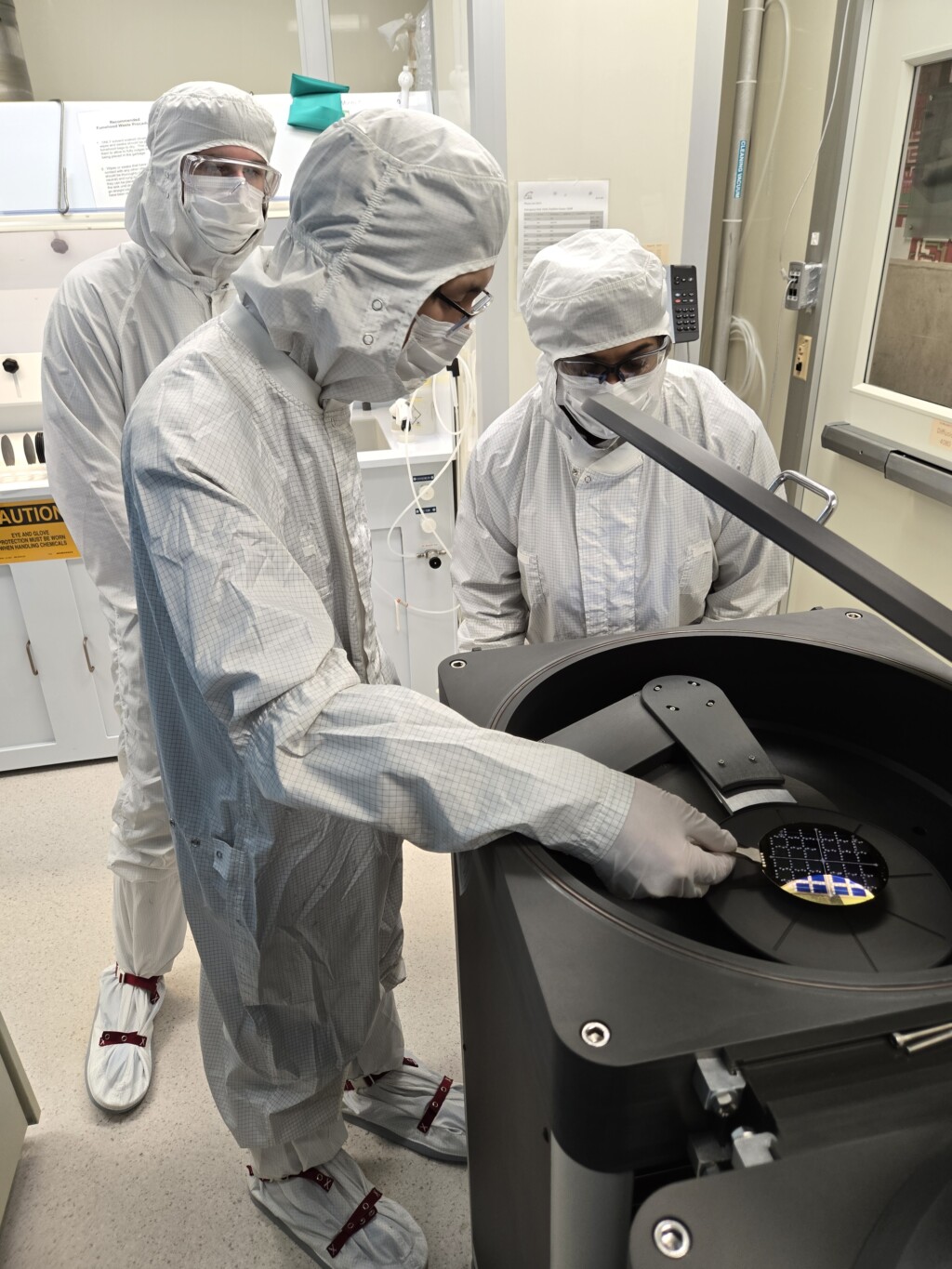
- Cleanroom environment and safety protocols in microfabrication (Emphasis on practical aspects and gowning procedures).
- Introduction to the Fab Lab facilities and equipment with detailed equipment demos.
Module 2: Schematic Capture with Cadence Virtuoso (Refresher & Project Setup)
Module 2: Schematic Capture with Cadence Virtuoso
- Quick refresher on using Cadence Virtuoso for schematic entry and design.
- Setting up the design project for the CMOS inverter and ring oscillator circuits to be fabricated.
- Library management and component selection relevant to the fabrication process.
Module 3: Circuit Simulation with Spectre (Focused on Performance Analysis)
- Brief review of circuit simulation principles and techniques.
- Using Cadence Spectre for simulation and performance analysis of the inverter and ring oscillator.
- Focus on key performance metrics relevant to fabricated devices (e.g., switching speed, power consumption).
- Analyzing simulation results and relating them to process parameters.
Week 2: Layout and Verification – Preparing for Mask Design
Module 4: Layout Design using Analog Artist (Hands-on Layout of Target Circuits)
- Review of IC layout design principles and design rules, tailored to the target fabrication process.
- Hands-on training on using Cadence Analog Artist for physical layout of the CMOS inverter and ring oscillator.
- Component placement, routing, and design rule checking (DRC).
- Understanding layout effects and parasitic extraction and their impact on circuit performance.
Module 5: Layout vs. Schematic (LVS) and Parasitic Extraction
- Importance of layout verification for design integrity.
- Using LVS tools to verify the consistency between schematic and layout of designed circuits.
- Identifying and correcting layout errors specific to microfabrication constraints.
- Introduction to parasitic extraction and its impact on simulated vs. fabricated circuit performance.
Week 3: Pre-Fabrication – Mask Design, Wafer Prep, and Advanced Cleanroom Protocols
Module 6: Mask Design and Preparation for Photolithography
- Understanding the role of masks in photolithography and mask fabrication process.
- Generating final mask layouts (GDSII) from verified CAD designs.
- Detailed design rule considerations and critical dimension control for mask fabrication and photolithography.
- Preparing design files for mask production and submission.
Module 7: Wafer Preparation and Characterization
- In-depth introduction to Silicon-On-Insulator (SOI) wafers and their advantages for this process.
- Detailed procedures for preparing SOI wafers (100nm Si film thickness) for fabrication processes, including cleaning and surface preparation.
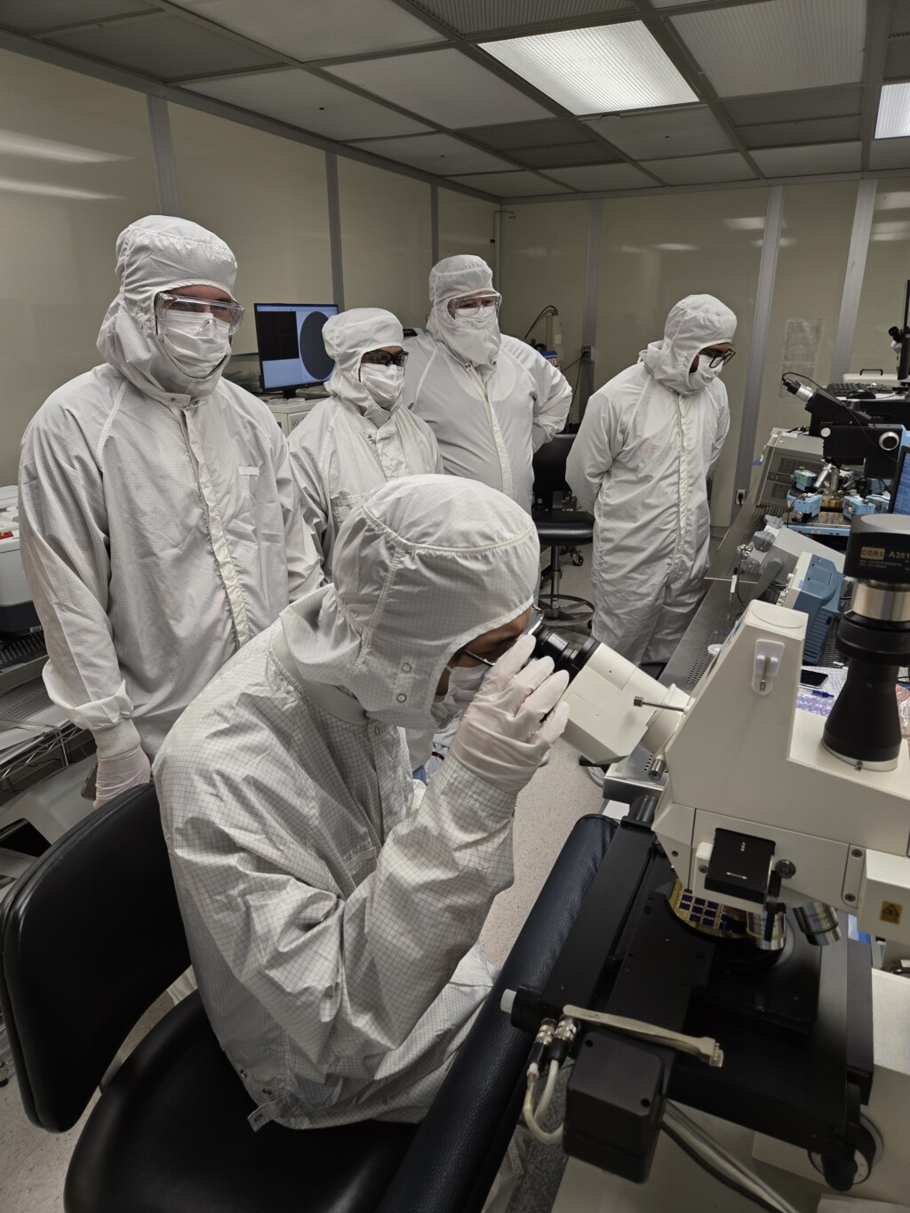
- Hands-on wafer cleaning and handling procedures in the cleanroom environment.
- Introduction to wafer characterization techniques: Ellipsometry for film thickness measurement, Profilometry for surface roughness. (Demonstration and data analysis).
Module 8: Advanced Cleanroom Protocols and Contamination Control
- In-depth training on advanced cleanroom protocols and best practices.
- Focus on contamination sources, particle control, and minimizing defects in microfabrication.
- Hands-on practice with advanced gowning techniques and cleanroom behavior for optimal fabrication outcomes.
Week 4: Fabrication Process – Photolithography, Oxidation and Polysilicon Deposition
Module 9: Patterning Device Well (PE1) – Photolithography and Etching
- Introduction to photolithography principles: Wave nature of light, diffraction, resolution limits.
- Hands-on experience with photoresist coating, soft bake, exposure using a stepper, post-exposure bake, and development.
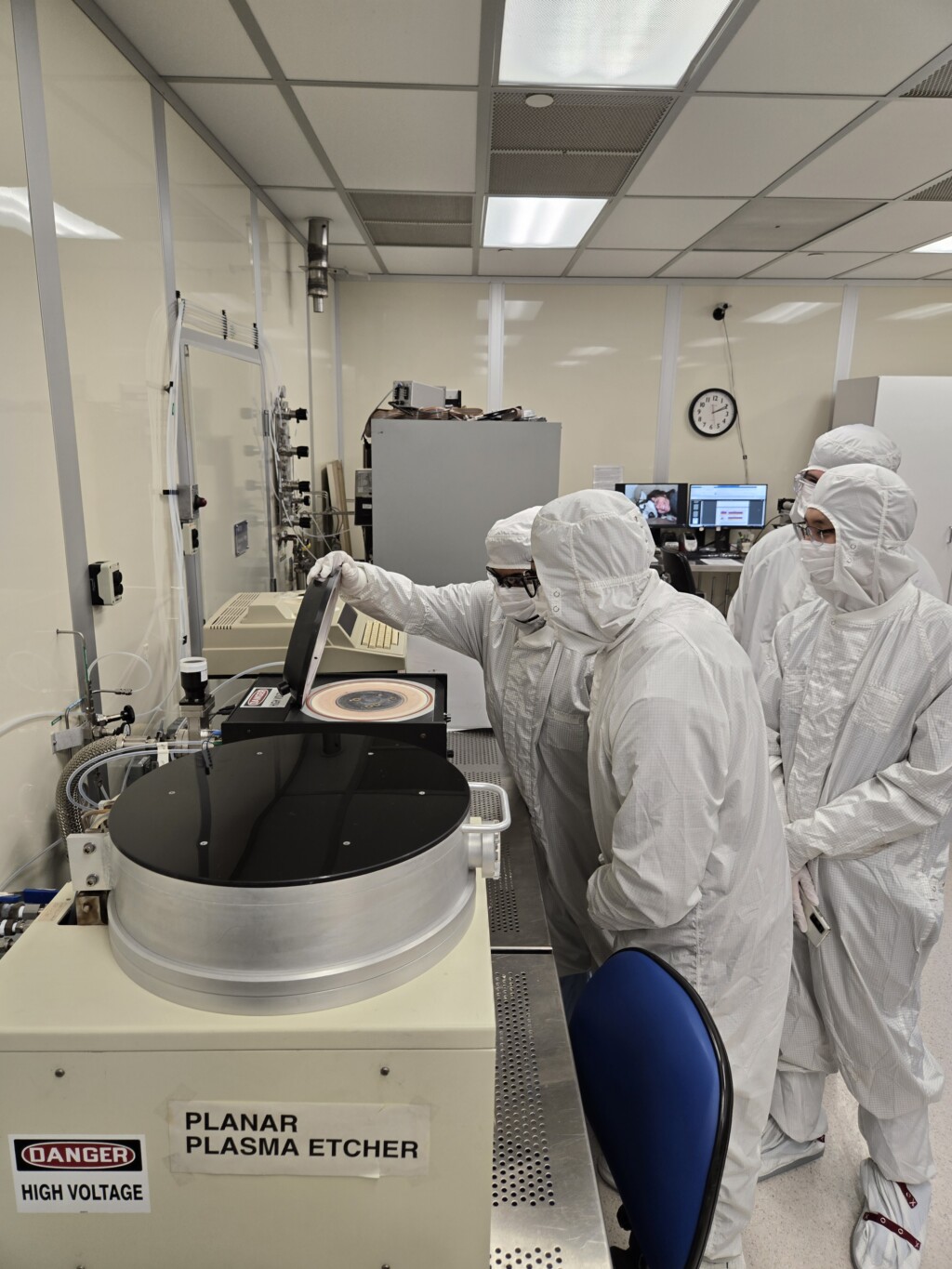
- Patterning device wells (PE1 layer) using photolithography and wet etching techniques (chemistry of silicon etching, selectivity).
- Cleanroom procedures and process control in photolithography and etching.
Module 10: Gate Oxide Growth (OX1) – Thermal Oxidation
- Introduction to thermal oxidation and its importance in MOSFET fabrication: Dry and wet oxidation, oxide growth kinetics (Deal-Grove model).
- Growing 25nm gate oxide (OX1 layer) at 950°C using thermal oxidation in a furnace.
- Understanding oxidation kinetics and factors affecting oxide quality (stress, interface traps).
- Safety protocols for high-temperature processes and gas handling.
Module 11: Polysilicon Deposition (PO) – Thin Film Deposition
- Introduction to thin film deposition techniques: Chemical Vapor Deposition (CVD) principles, different CVD methods (LPCVD).
- Depositing 350nm polysilicon (PO layer) for gate electrode formation using LPCVD.
- Understanding film properties (stress, uniformity, conformality) and deposition parameters (temperature, pressure, gas flow rates).
Week 5: Fabrication Process – Doping, Implantation, and Dielectric Deposition
Module 12: NMOS and PMOS Poly Layers Patterning (PP, PN) – Doping and Implementation
- Introduction to semiconductor doping and ion implantation: Diffusion and ion implantation mechanisms, doping profiles, junction formation.
- Patterning nMOS and pMOS poly layers (PP, PN layers) using photolithography and etching.
- Diffusion of phosphorus for n-type doping and ion implantation of boron for p-type doping (dopant diffusion profiles, activation annealing).
- Understanding doping profiles and junction formation and their impact on transistor characteristics.
Module 13: BPSG Deposition and Open Contact Windows (PE4) – Dielectric Deposition and Etching
- Introduction to dielectric materials and their role in ICs: Properties of dielectrics, interlayer dielectrics (ILDs).
- Depositing Borophosphosilicate Glass (BPSG) as an interlayer dielectric using CVD.
- Opening contact windows (PE4 layer) using photolithography and dry etching techniques (plasma etching principles, anisotropy) to access underlying layers.
- Planarization techniques and via formation and their importance for multi-layer interconnects.
Module 14: Metal Deposition and Patterning (PE5) – Metallization and Final Fabrication Steps
- Introduction to metallization for interconnects in ICs: Sputtering and other metallization techniques, properties of metals for interconnects (conductivity, electromigration).
- Performing metal deposition and patterning (PE5 layer) for final interconnections using sputtering and photolithography/etching.
- Final fabrication steps, wafer dicing, and basic die separation.
- Device packaging and encapsulation (overview and industry examples).
Week 6: Testing Phase – Characterization, Yield Analysis, and Industry Perspectives
Model 15: Probe Testing and Characterization of Fabricated ICs
- Setting up probe testing station with up to 6 probes.
- Performing DC electrical measurements on fabricated CMOS inverters: Transfer characteristics, threshold voltage extraction, noise margin analysis.
- Measuring AC performance of ring oscillators: Gate delay, frequency of oscillation.
- Circuit-specific functional testing and verification.
Module 16: Performance Characterization, Yield Analysis, and Process Parameter Extraction
- Analyzing test data and performing performance characterization of fabricated devices.
- Introduction to yield analysis and statistical process control (SPC) in IC manufacturing.
- Factors affecting IC yield: Defect density, process variations.
- Process parameter extraction from electrical measurements: Mobility, sheet resistance, oxide thickness (using simplified models).
- Documentation of results and report writing.
Module 17: Industry Mixer Event and Networking & Advanced Characterization Techniques (Overview)
- Networking session with industry leaders from companies like Nokia, TSMC, and Marvell (or similar industry partners).
- Industry insights and career perspectives in semiconductor technology.
- Q&A and interaction with industry professionals.
- Brief overview of advanced characterization techniques for process and device analysis: Scanning Electron Microscopy (SEM), Transmission Electron Microscopy (TEM), Atomic Force Microscopy (AFM) – principles and applications in IC fabrication.
Final Assessment and Course Conclusion
- Final assessment includes performance characterization, yield analysis, and documentation of results in a short report.
- Course wrap-up, feedback, and certificate distribution.
Course Fees & Prospective Student Timelines
All course fees and costs are in Canadian (CAD) dollars
- Application Processing Fee: $100 (non-refundable), payable at registration
- Course Fee: $6,850
This is a high sought-after limited-enrollment course. Prospective students are encouraged to register early to secure their spot. The following timeline outlines key dates, fees, and activities for prospective students.
| Fee (CAD) | Date (Approximate) | Activity/Deliverable |
|---|---|---|
| $100 | April 15, 2025 | Application Deadline |
| March 2025 (last week) | First Information Session (Online) | |
| April 2025 (1st week) | Second Information Session (Online) | |
| April 1 – April 20, 2025 | Prospective Student Interviews and selection confirmation | |
| $3,425 | April 25, 2025 | First installment of course fee (refundable in case of Visa denial) |
| April 22, 2025 | Third Information Session (Visa Focus) | |
| $3,425 | May 30, 2025 | Second installment of course fee (Remaining Balance) |
| June 2025 (1st Week) | Fourth Information Session (Onboarding) | |
| June 16 – July 25, 2025 | 6-Week Course (In Person) | |
| End of Course (July 25, 2025) | Submission of Final Report, Certificate Distribution |
Additional Highlights
- Master’s Pathway Program: Streamlined admission and potential fee waivers for Carleton University’s Electrical Engineering graduate programs including MASc, MEng, and Engineering Practice.
- Key Process Training: Wafer Preparation, Photolithography, Thermal Oxidation, Chemical Vapor Deposition, Ion Implantation, Metallization.
- Optional University Credit: Opportunity to earn 0.5 university credit applicable towards future graduate studies at Carleton University (additional fee of $3,000).
- Intensive Training: Courses on VLSI Design, Semiconductor Devices, IC Fabrication, and IC Testing.
- Industry Mixer Events: Network with leaders from Nokia, TSMC, and Marvell.
- Academia Mixer Events: Network with Carleton University professors and graduate students.
- State-of-the-Art Tools: Learn analog IC design and layout using industry-standard CAD tools from Cadence (Virtuoso, Spectre, Analog Artist).
Accommodation and Meals (Optional, Student Responsibility, Purchased Separately)
All accommodation fees and costs are in Canadian (CAD) dollars
Availability: Offered through Carleton University Conference Services.
Room Options & Rates (per person, per night):
- Traditional: Traditional style residences consist of two single beds and desks per room that share a washroom with the adjoining room. Rate: $40.00/person/night + 15% housing administration charge. Note: Private rooms are not available at this rate. Estimated Cost (6 weeks): ~ $1,932.
- Suite: Suite style residences consist of two or four bedrooms, each furnished with one double bed and a desk, which share a common area equipped with a microwave and fridge, and a private washroom. Rate: $65.00/person/night + 15% housing administration charge. Note: Private suites are not available at this rate. Estimated Cost (6 weeks): ~ $3,140.
- Check-in/Check-out: Check-in is any time after 3:00pm and check-out is before 11:00am.
Meal Plans:
- Availability: All-you-care-to-eat meals are available at “The Caf” (Carleton University’s main cafeteria).
- Meal Rates
- Full Meal Plan (Breakfast, Lunch, and Dinner, all-you-can-eat): Estimated Cost $56/day (6 weeks: ~ $2,355) inclusive of all taxes and fees.
Important Notes:
- All accommodation and meal plan costs are estimates based on current pricing from Carleton University Conference Services and are subject to change.
- Accommodation and meal plans must be booked separately by the student directly through Carleton University Conference Services (or an alternative provider, if the student plans on using alternative options).
- Accommodation availability at Carleton University is subject to blackout dates and early booking is strongly recommended.
The course organizers do NOT cover the costs of travel, health insurance, accommodation, food, or any other related expenses. Associated arrangements and costs are the responsibility of the students.
In summary, the total estimated cost is $6,950 (application + course fee) + $1,932 (accommodation) + $2,355 (meal plan) = $11,237 CAD which is approximately 6.9 Lakhs in INR at the current exchange rate. Additional costs such as airfare, visa fees, and personal expenses are the student’s responsibility.
The application link below will take you to a form on a new page. Please complete the form to confirm your interest and begin the application process.
Application Form for Carleton IC Fabrication Training Program
Note: For those having any constraint in taking the currently offered course (such as with the dates of the program, duration of the program), please feel free to contact the department with your input. The department will consider the possibility of accommodating these inputs based on the available resources and scheduling constraints..