Carleton University Microfabrication Facility (CUMFF)
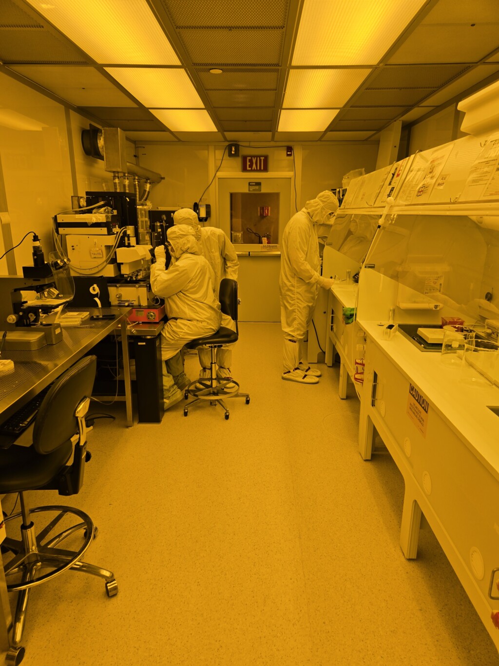
The Carleton University MicroFabrication Facility is a class 100 – 10,000 – 3200 square foot cleanroom facility used for manufacturing silicon integrated circuits and other device materials in support of research on:
- Process technology
- Device physics/modeling
- Innovative circuit techniques
- Photonics
- Biomedical devices
- Renewable energy (solar cells)
- Micro-electromechanical systems (MEMS)
External academic and industrial users/partners are also welcome to access the lab and equipment for research work, small-volume production runs or start-up processing.
MOS Processing
MOS gate dielectrics can be produced with contamination at industry acceptable levels. To illustrate this capability, every year the CUMFF lab is used in a quasi-production mode to fabricate student submitted designs on a multi-project chip from layout to completed chip.
The project uses 5µm LOCOS-isolated polysilicon gate nMOS technology and more recently cMOS technology on SOI material. The working chips are returned for testing within 3 weeks of submission of CAD files, and wafer-level probing usually indicates yields of over 80% for the circuits.
Facility Layout
The lab contains 4 distinct working areas for:
- Photolithography
- Metrology area
- Furnace operations
- High vacuum processes
A separate air conditioning system maintains the facility temperature at 20 degrees Celsius with 40% relative humidity throughout the entire year. Class 100 air quality is maintained in the photolithography and photomask production areas (approximately 80 m2 total), Class 1,000 in the vacuum system area and class 10,000 in the oxidation/diffusion area.

Access for External Users
External users may access the MFF for research work or small-volume production runs subject to the availability of resources and the recovery of operating costs. In the recent past the facility has carried out contract production of solar cells and MOSFET-based gamma ray dosimeters.
Further information on availability and cost may be obtained from facility manager Rob Vandusen.
Fees
Microfabrication Lab Subscription Plans
Access
For lab access please contact the facility manager Rob Vandusen and include the details of your research requirements.
Once lab users complete the prerequisite training they will be provided access to the lab and the NEMO Lab Management system. Here, they can view and book lab equipment, contact the lab staff, view safety and equipment training manuals along with other resources.
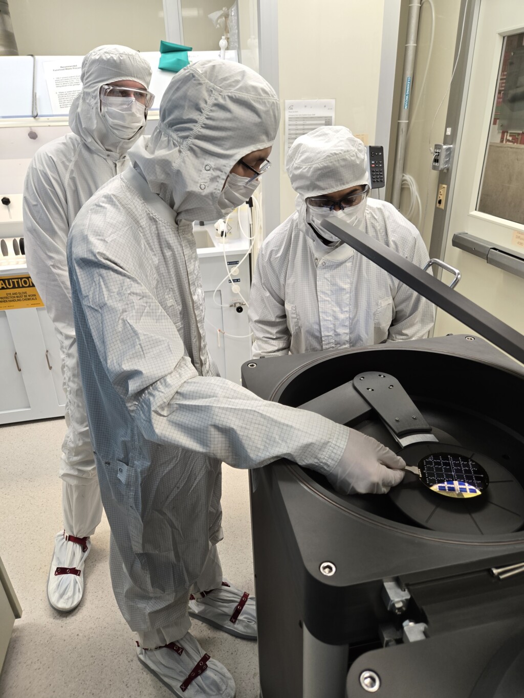
Hands-on Microfabrication for Integrated Circuits – Short Course Information
The Department of Electronics is offering a comprehensive 6-week fabrication short course – Hands-on Microfabrication for Integrated Circuits – which bridges the gap between theoretical knowledge and practical application in semiconductor technology.
Recent Research Projects
Professor Shulabh Gupta‘s NSERC/Mitacs-funded project aims to develop smart electromagnetic (EM) refractor and reflector surfaces operating in strategic millimeter-wave (mmWave) and optical frequency bands, enabling real-time beamforming for 5G and beyond wireless communication systems as well as holographic applications.
In collaboration with Dell Canada, the project explores the use of advanced electromagnetic materials to design metasurface refractors that are optically transparent yet active at mmWave frequencies. Materials such as grapheneand tunable dielectrics are investigated for their electronically tunable properties, allowing precise control within metasurface structures.
Unlike conventional hybrid fabrication methods that rely on off-the-shelf components, this project focuses on monolithic integration of advanced materials directly into resonator arrays, enabling compact and efficient metasurface designs. The initial phase includes detailed material and device characterization across selected frequency bands, followed by co-design of metasurface resonator particles for tailored beamforming behavior.
The project also involves the development of novel microfabrication techniques, scaling from small-scale device prototypes to large-area surface implementations, including the integration of electronic biasing networks for dynamic control.
The resulting mmWave metasurfaces will act as “smart windows” for radio environment engineering, improving wireless signal coverage across multiple rooms. These innovations aim to deliver high-speed connectivity in urban areas and robust point-to-point links in rural and remote communities, helping bridge the digital divide in Canada.
Overall, this initiative strengthens Canada’s position in the wireless technology landscape, advancing metamaterials science through academic-industry collaboration, and contributing to next-generation digital infrastructure.
Photolithography
- Photolithography is carried out using a Karl-Suss MA6 UV mask aligner, which can accept substrates ranging from small fragments to 100mm diameter wafers.
- Feature sizes down to 0.8µm have been printed using chrome masks.
- A HMDS vapor oven, photoresist spinners, bake ovens, hotplates and developing benches are used for the photoresist processing.
Oxidation/Diffusion
- An eight-stack Bruce Model BDF-8 furnace bank is available for thermal processing up to 1200 C on wafers up to 100 mm in diameter.
- Tubes for oxidation, implant annealing and drive-in, phosphorus predeposition and hydrogen metal sinter are operational.
- Gettering with HCl gas is used before all oxidation cycles to control Na+ ionic contamination. With this precaution it is possible to produce gate oxides showing effectively no flatband shift in bias-temperature stress tests.
LPCVD/PECVD
- A four-stack Bruce furnace bank is used for Low Pressure Chemical Vapor Deposition.
- Depositions include:
- LPCVD Oxides (doped and undoped)
- BPSG
- Amorphous Silicon and PoySilicon, and Silicon Nitride
- A Trion Orion III PECVD system used for PECVD Silicon Nitride, Silicon dioxide and hydrogenated silicon films on up to 8″ wafers.
Cleaning and Wet Etching
- Several wet benches with exhaust and cascade rinsers are available throughout the lab for wet chemical processing and cleaning.
- Ultrapure18 Mega ohm DI (De-ionized) water is produced onsite, stores in a 200 gallon tank and continuously re-circulated throughout the lab to maintain purity
- Clean DI water is essential for the production of semiconductor devices.
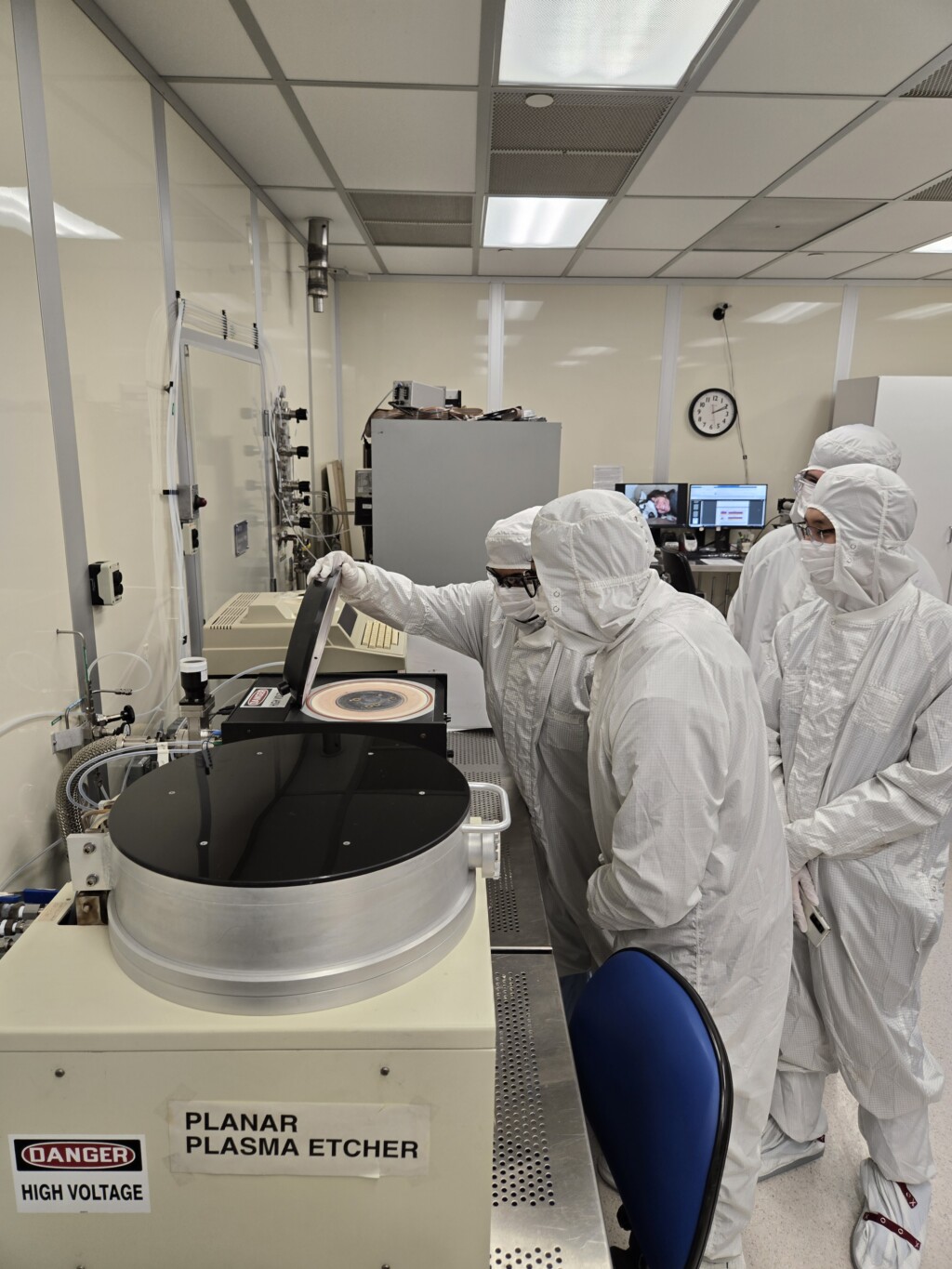
Plasma Etching
- Several dry etch systems are available in the Microfabrication lab:
- A MRC RIE 61 reactive ion etcher is used for oxide etching, including sidewall spacer formation
- Vertical-walled optical waveguides 10 µm high have been etched in deposited SiO2 layers to form optical waveguides.
- Other plasma etch systems include a Technics Planar Etch II ,a March RIE etcher and 2 microwave plasma etchers for resist stripping.
Metallization and Thin Films
- Several multi-purpose metal deposition systems are available:
- A loadlocked inline Semicore sputtering system with sputter etch capability
- Two ebeam/thermal evaporator systems
- A Varian M2000 single chamber RF/DC sputter system
- A number of different materials can be deposited including Al, Ti, Au, Ag, SiO2, Cr, Pt etc.
- Access to Atomic Layer Deposition processing (ALD), is available through the newly opened Facility for Nanostructures, Surfaces, and Sensor Interfaces (FANSSI) facility on the 5th floor of the Minto Building.
- This new Chemistry/Electronics shared facility includes a wetlab and a class 10,000 cleanroom lab. The equipment set includes a Picosun Atomic Layer deposition system, a Angstrom Engineering Thermal Evaporation system housed inside a Mbraun high purity glovebox, and a Trion PECVD system.
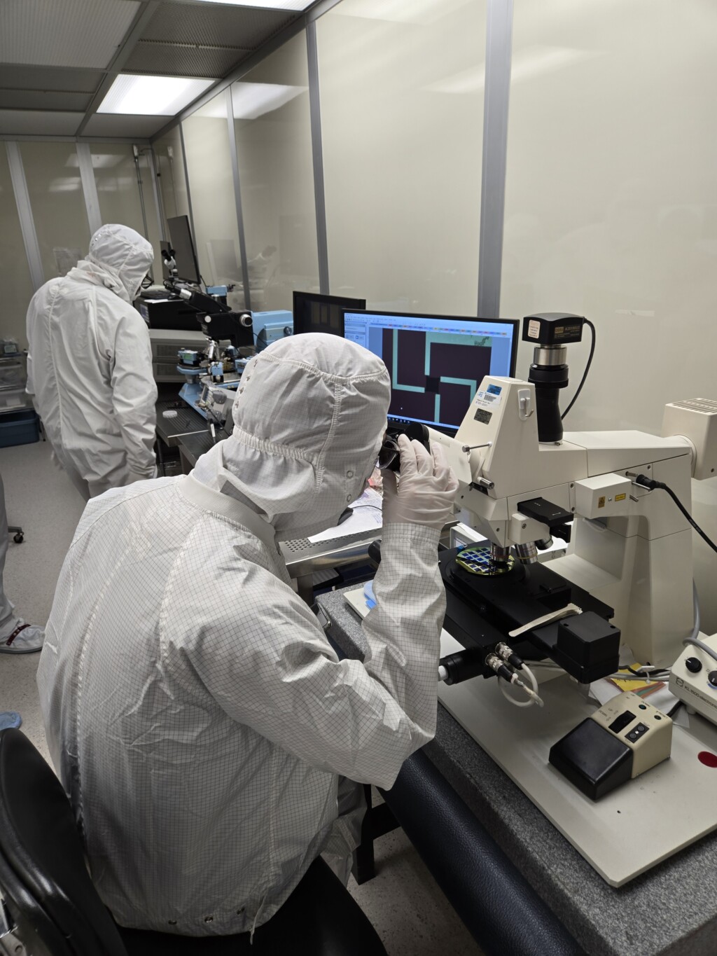
Process Monitoring
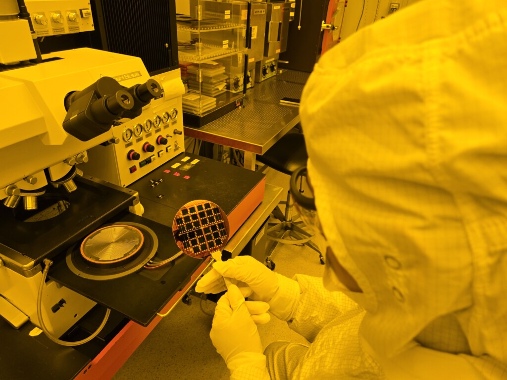
- Optical microscopes are available throughout the lab for optical inspections, taking photographs and making linewidths measurements if necessary.
- Ellipsometers, profilometers, and an AFM Atomic Force Microscope are available for film thickness and characterization.
- A Jeol Scanning electron microscope is available for SEM imaging.
- A CV test station consisting of a hot chuck with a CV meter is available to test gate dielectric quality.
Dicing/Wirebonding/Testing
- Wafer dicing, wirebonding and testing equipment is also available for non-production type projects.